



Ten years ago, France said no. India had asked for access to gallium nitride, or GaN, technology as part of the offsets in the 2016 Rafale fighter jet deal, and Paris decided the technology was too sensitive to share. This week, reports confirmed that India no longer needs to ask. The Defence Research and Development Organisation has built an indigenous GaN capability for military radars and electronic warfare, turning a decade-old refusal into a domestic success story.
The development, reported on November 6 and 7, rests on work by two DRDO-linked laboratories: the Solid State Physics Laboratory (SSPL) in Delhi and the Gallium Arsenide Technology Enabling Centre (GAETEC) in Hyderabad. Together, they have given India the ability to make GaN-based High Electron Mobility Transistors (HEMTs) and Monolithic Microwave Integrated Circuits (MMICs), the building blocks of modern radar.
Why GaN matters for fighter jets
GaN is the material at the heart of the latest generation of military radar. Compared with the older gallium arsenide technology, it handles far higher power, runs cooler and works at higher frequencies. For a fighter jet, that means a radar that can see farther, track more targets and resist jamming better.
The most important application is the Active Electronically Scanned Array, or AESA, radar. In an AESA system, hundreds of small transmit-receive modules work together to steer the radar beam electronically, with no moving parts. GaN makes those modules more powerful and more compact, which is exactly what a modern fighter needs.
India’s most visible GaN project is the Virupaksha radar, being developed for the Indian Air Force’s Su-30MKI fleet. The radar, built on GaN technology, saw its first power-on test in February 2026.
From 2024 capability to 2026 showcase
The breakthrough did not arrive overnight. In November 2024, the Ministry of Defence announced that SSPL had developed indigenous processes to manufacture four-inch silicon carbide wafers and GaN-based HEMTs with power handling of up to 150 watts. The laboratory had also built GaN-based MMICs delivering up to 40 watts. GAETEC, meanwhile, established limited production capability for GaN-on-SiC MMICs.
At ESTIC 2026, held at Bharat Mandapam from October 27 to 29, DRDO put that work on public display. SSPL presented GaAs and GaN-based MMICs and multi-chip modules, alongside infrared focal plane arrays that serve as the eyes of tactical missiles. The message was plain: the chips that once had to be imported are now being made in Indian laboratories.
How the chips are made
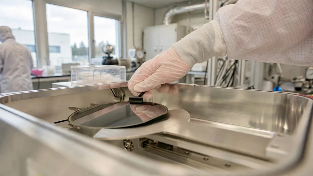
- Material growth: GaN layers are deposited on specialised substrates using Metal Organic Chemical Vapour Deposition (MOCVD), a process that demands precise control of gas purity, crystal structure and layer thickness.
- Transistors: SSPL fabricates GaN HEMTs that can handle up to 150 watts of power, far beyond what older materials manage.
- Integrated circuits: GaN MMICs pack amplifiers and switches onto a single chip, delivering up to 40 watts for radar transmit-receive modules.
- Production base: GAETEC in Hyderabad has set up limited production capability for GaN-on-SiC MMICs, moving the technology from laboratory to factory floor.
The private sector joins in
The GaN story is not limited to government laboratories. In December 2023, the Ministry of Defence signed an iDEX contract with Bengaluru-based Agnit Semiconductors to develop advanced GaN semiconductors for defence transmitters, radars and electronic warfare equipment. The Indian Institute of Science, through its Centre for Nano Science and Engineering, has developed GaN device fabrication techniques using specialised facilities.
The wider semiconductor ecosystem is moving in the same direction. The Union Cabinet approved the next phase of the India Semiconductor Mission, Semicon 2.0, on July 15, 2026, with an outlay of Rs 1,27,500 crore.
What it means for India’s defence
Self-reliance in GaN removes a strategic vulnerability. Radars and electronic warfare systems sit at the centre of modern air combat, and dependence on foreign suppliers for their core chips would leave every upgrade and repair at the mercy of export controls. Building the capability at home means the Air Force’s AESA upgrades, from the Su-30MKI’s Virupaksha radar to future indigenous fighters, can proceed on India’s own timetable.
There are limits to be honest about. Reports note that Indian GaN work still relies on some imported materials and fabrication equipment, and production volumes remain modest compared with global leaders. The achievement is real, but it is a foundation, not a finished industry.
FAQs
What are GaN chips?
Gallium nitride chips are semiconductors used in high-power, high-frequency electronics. In defence, they power the transmit-receive modules of AESA radars and electronic warfare systems.
Why did France refuse GaN technology to India in 2016?
India sought access to GaN technology as part of the offsets in the Rafale deal. According to a report by The Week in January 2026, French authorities considered it too sensitive to transfer.
Which Indian laboratories developed the GaN capability?
DRDO’s Solid State Physics Laboratory in Delhi and the Gallium Arsenide Technology Enabling Centre in Hyderabad, with support from IISc and private firms like Agnit Semiconductors.
What is the Virupaksha radar?
It is an indigenous GaN-based AESA radar being developed for the Indian Air Force’s Su-30MKI fighter fleet. It saw its first power-on test in February 2026.
How powerful are India’s GaN devices?
SSPL’s GaN HEMTs handle up to 150 watts, and its GaN MMICs deliver up to 40 watts, according to the Ministry of Defence announcement of November 2024.
India’s GaN journey shows what a refused technology transfer can become: not a dead end, but a deadline. The chips are here and the radar is being tested.